- 您现在的位置:买卖IC网 > Sheet目录346 > NCV8855BMNR2GEVB (ON Semiconductor)BOARD EVALUATION NCV8855 ASIC
�� �
�
�NCV8855�
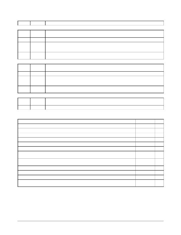
�PIN� FUNCTION� DESCRIPTIONS�
�Pin� No.�
�Symbol�
�Description�
�LOW� DROPOUT� LINEAR� REGULATOR� CONTROLLER� 1� (LDO1)� PIN� CONNECTIONS�
�38�
�1�
�40�
�39�
�LR_FB1�
�LR_G1�
�ISNS1+�
�ISNS1� ?�
�LDO� controller� output� voltage� feedback� pin.� Connect� a� resistor� divider� network� to� VOUT3� to� set� the� desired�
�output� voltage.�
�Error� amplifier� output� of� the� LDO� controller.� Connect� to� gate� of� P� ?� Channel� MOSFET� pass� element.�
�Current� sense� positive� input.� Connect� this� pin� to� the� supply� side� of� the� current� sense� resistor.� This� pin� also�
�serves� as� the� supply� rail� for� the� linear� regulator� controller.� A� local� bypass� capacitor� with� a� value� of� 0.1� m� F� to� 1�
�m� F� is� recommended.�
�Current� sense� negative� input.� When� using� a� current� sense� resistor,� connect� this� pin� to� the� pass� element� side�
�of� the� current� sense� resistor.� If� current� limit� is� not� used,� connect� this� pin� to� the� supply� rail� of� the� pass� element.�
�LOW� DROPOUT� LINEAR� REGULATOR� CONTROLLER� 2� (LDO2)� PIN� CONNECTIONS�
�34�
�33�
�31�
�32�
�LR_FB2�
�LR_G2�
�ISNS2+�
�ISNS2� ?�
�LDO� controller� output� voltage� feedback� pin.� Connect� a� resistor� divider� network� to� VOUT3� to� set� the� desired�
�output� voltage.�
�Error� amplifier� output� of� the� LDO� controller.� Connect� to� gate� of� P� ?� Channel� MOSFET� pass� element.�
�Current� sense� positive� input.� Connect� this� pin� to� the� supply� side� of� the� current� sense� resistor.� This� pin� also�
�serves� as� the� supply� rail� for� the� linear� regulator� controller.� A� local� bypass� capacitor� with� a� value� of� 0.1� m� F� to� 1�
�m� F� is� recommended.�
�Current� sense� negative� input.� When� using� a� current� sense� resistor,� connect� this� pin� to� the� pass� element� side�
�of� the� current� sense� resistor.� If� current� limit� is� not� used,� connect� this� pin� to� the� supply� rail� of� the� pass� element.�
�HIGH� ?� SIDE� LOAD� SWITCH� (HSS)� PIN� CONNECTIONS�
�26�
�28�
�VIN�
�HS_S�
�This� pin� is� the� supply� rail� for� the� internal� high� ?� side� load� switch,� DRV_VPP� and� 5V_IC.� Bypass� this� pin� with� a�
�1� m� F� ceramic� capacitor.�
�Source� node� output� of� the� internal� high� ?� side� N� ?� Channel� MOSFET� load� switch.�
�MAXIMUM� RATINGS� (Voltages� are� with� respect� to� AGND� unless� noted� otherwise)�
�Pin� Name�
�Max� dc� voltage� (GH1,� BST1,� SN1,� SN2,� BST2,� HS_S)�
�Negative� Transient� (t� <� 50� ns)� (SN1,� SN2)�
�Max� dc� voltage:� 5V_IC�
�Max� dc� voltage:� DRV_VPP�
�Max� dc� voltage� (BST1� &� GH1w/respect� to� SN1,� GL1,� BST2� w/respect� to� SN2)�
�Max� dc� voltage� (OCSET,� ISNS1+,� ISNS1� ?� ,� LR_G1,� VIN,� VIN_SW,� ISNS2+,� ISNS2� ?� ,� LR_G2)�
�Peak� Transient� (ES� ?� XW7T� ?� 1A278� ?� AB� Test� Pulse� G� –� Loaded� Conditions)�
�(OCSET,� ISNS1+,� ISNS1� ?� ,� LR_G1,� VIN,� VIN_SW,� ISNS2+,� ISNS2� ?� ,� LR_G2)�
�Max� dc� voltage� (SW_FB1,� COMP1,� LR_FB1,� LDO_EN,� HOT_FLG,� SW_FB2,� COMP2,� LR_FB2,� HS_EN,�
�SYS_EN,� SYNC)�
�Max� dc� voltage:� PGND�
�Maximum� Operating� Junction� Temperature� Range,� T� J�
�Maximum� Storage� Temperature� Range,� T� STG�
�Peak� Reflow� Soldering� Temperature:� Pb� ?� Free�
�60� to� 150� seconds� at� 217� °� C�
�Value�
�?� 0.3� to� 30�
�?� 2�
�6�
�9�
�?� 0.3� to� 15�
�?� 0.3� to� 40�
�?� 0.3� to� 45�
�?� 0.3� to� 7�
�?� 0.3� to� 0.3�
�?� 40� to� 150�
�?� 55� to� +150�
�260� peak�
�Unit�
�V�
�V�
�V�
�V�
�V�
�V�
�V�
�V�
�V�
�°� C�
�°� C�
�°� C�
�Stresses� exceeding� Maximum� Ratings� may� damage� the� device.� Maximum� Ratings� are� stress� ratings� only.� Functional� operation� above� the�
�Recommended� Operating� Conditions� is� not� implied.� Extended� exposure� to� stresses� above� the� Recommended� Operating� Conditions� may� affect�
�device� reliability.�
�http://onsemi.com�
�4�
�发布紧急采购,3分钟左右您将得到回复。
相关PDF资料
NCV8871BSTGEVB
BOARD EVAL NCV8871BST BOOST CTLR
NHC-14150
VALULINE 8" X 8.5" X 1.75"
NHC-14151
VALULINE 8" X 17" X 1.75"
NHC-14152
VALULINE 13" X 17" X 1.75"
NHC-14153
VALULINE 8" X 8.5" X 3.5"
NHC-14154
VALULINE 8" X 17" X 3.5"
NHC-14155
VALULINE 13" X 17" X 3.5"
NHC-14156
VALULINE 13" X 17" X 5.25"
相关代理商/技术参数
NCV8870
制造商:ONSEMI 制造商全称:ON Semiconductor 功能描述:Automotive Grade Non-Synchronous Boost Controller
NCV887000
制造商:ONSEMI 制造商全称:ON Semiconductor 功能描述:Automotive Grade Non-Synchronous Boost Controller
NCV887000D1R2G
功能描述:低压差稳压器 - LDO Auto Grade Non-Sync Boost Controller
RoHS:否 制造商:Texas Instruments 最大输入电压:36 V 输出电压:1.4 V to 20.5 V 回动电压(最大值):307 mV 输出电流:1 A 负载调节:0.3 % 输出端数量: 输出类型:Fixed 最大工作温度:+ 125 C 安装风格:SMD/SMT 封装 / 箱体:VQFN-20
NCV887001
制造商:ONSEMI 制造商全称:ON Semiconductor 功能描述:Automotive Grade Non-Synchronous Boost Controller
NCV887001D1R2G
功能描述:低压差稳压器 - LDO Auto Grade Non-Sync Boost Controller
RoHS:否 制造商:Texas Instruments 最大输入电压:36 V 输出电压:1.4 V to 20.5 V 回动电压(最大值):307 mV 输出电流:1 A 负载调节:0.3 % 输出端数量: 输出类型:Fixed 最大工作温度:+ 125 C 安装风格:SMD/SMT 封装 / 箱体:VQFN-20
NCV887100D1R2G
功能描述:DC/DC 开关控制器 AUTOMOTIVE-GRADE NON-SYNC RoHS:否 制造商:Texas Instruments 输入电压:6 V to 100 V 开关频率: 输出电压:1.215 V to 80 V 输出电流:3.5 A 输出端数量:1 最大工作温度:+ 125 C 安装风格: 封装 / 箱体:CPAK
NCV887101D1R2G
功能描述:IC REG CTRLR BST PWM CM 8-SOIC RoHS:是 类别:集成电路 (IC) >> PMIC - 稳压器 - DC DC 切换控制器 系列:- 产品培训模块:Lead (SnPb) Finish for COTS
Obsolescence Mitigation Program 标准包装:2,500 系列:- PWM 型:电流模式 输出数:1 频率 - 最大:275kHz 占空比:50% 电源电压:18 V ~ 110 V 降压:无 升压:无 回扫:无 反相:无 倍增器:无 除法器:无 Cuk:无 隔离:是 工作温度:-40°C ~ 85°C 封装/外壳:8-SOIC(0.154",3.90mm 宽) 包装:带卷 (TR)
NCV887102D1R2G
功能描述:IC REG CTRLR BST PWM CM 8-SOIC RoHS:是 类别:集成电路 (IC) >> PMIC - 稳压器 - DC DC 切换控制器 系列:- 产品培训模块:Lead (SnPb) Finish for COTS
Obsolescence Mitigation Program 标准包装:2,500 系列:- PWM 型:电流模式 输出数:1 频率 - 最大:275kHz 占空比:50% 电源电压:18 V ~ 110 V 降压:无 升压:无 回扫:无 反相:无 倍增器:无 除法器:无 Cuk:无 隔离:是 工作温度:-40°C ~ 85°C 封装/外壳:8-SOIC(0.154",3.90mm 宽) 包装:带卷 (TR)